Understanding AI-Driven Parametric Design for Electronics
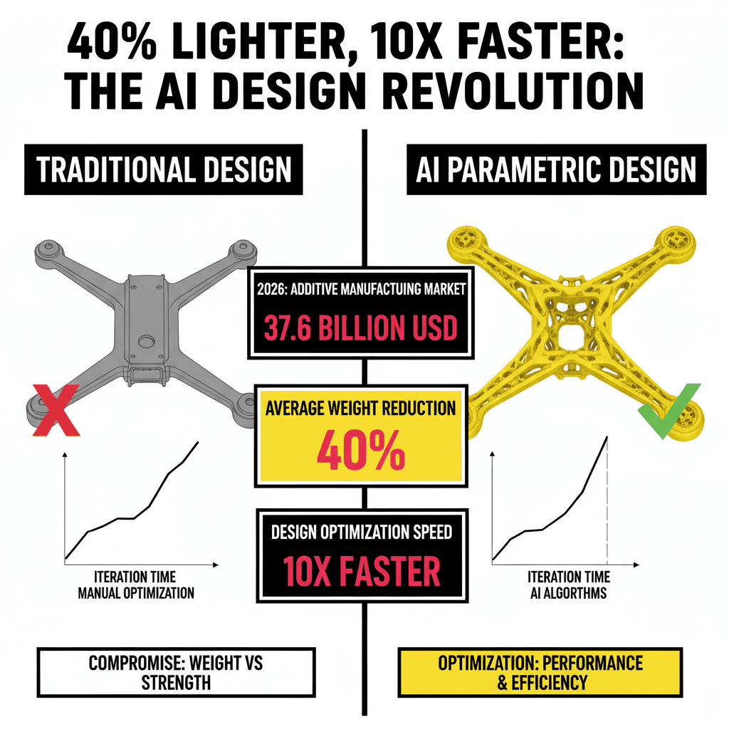
Parametric design represents a fundamental shift from traditional drawing to rule-based modeling. Instead of manually sketching every line, you define a set of parameters—dimensions, material properties, and load constraints—that dictate the final shape. Artificial intelligence has accelerated this process by automating the search for optimal geometry. In 2026, designers no longer guess which structure provides the best strength-to-weight ratio. AI algorithms now evaluate thousands of iterations per second to find the most efficient path for a 3D-printable component.
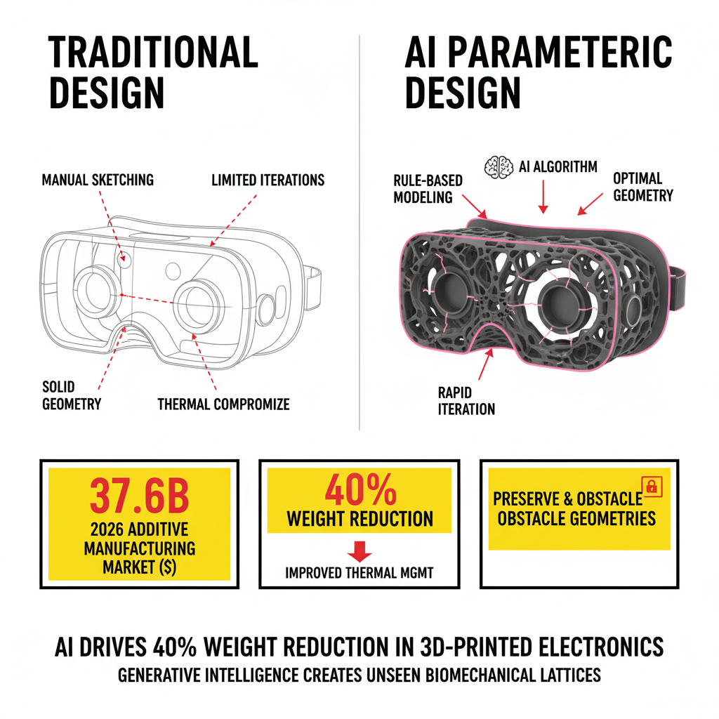
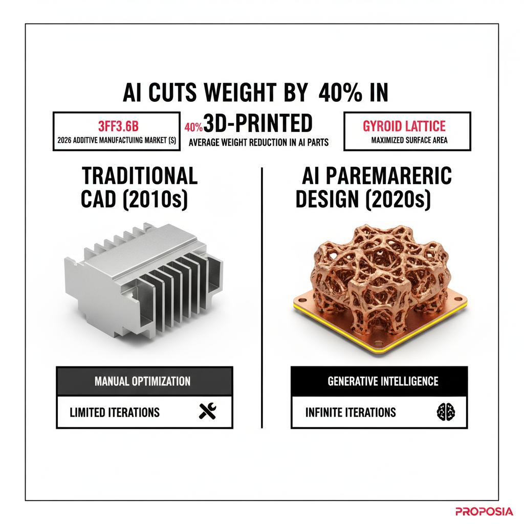
Consumer electronics require a delicate balance of aesthetics, durability, and thermal management. Traditional manufacturing often forces engineers to compromise, using solid blocks of plastic or metal that add unnecessary weight. AI-driven parametric design enables the creation of complex internal lattices that remain impossible to produce with injection molding. These structures can specifically target areas of high stress while leaving non-critical regions hollow or lightweight. Modern software integrates these capabilities directly into the design environment, making advanced engineering accessible to beginners.
Setting Your Design Constraints and Goals
The success of an AI-optimized part depends entirely on the data you provide at the start. Beginners must learn to translate physical requirements into digital constraints. If you are designing a drone frame, your primary goal might be weight reduction to extend battery life. For a high-end smartphone case, impact resistance and grip texture take priority. Designers specify these needs by defining "preserve geometries"—areas that cannot change, like screw holes or button openings—and "obstacle geometries" that the AI must avoid, such as the internal battery space.
Load cases are the next critical step in the setup process. You must tell the software where forces will be applied during real-world use. Imagine a handheld gaming console being dropped or squeezed. By applying these virtual forces to the model, the AI can reinforce the structure exactly where it expects failure. This data-driven approach ensures that the final 3D-printable product is not just lighter but also more reliable than a manually designed counterpart. Observe that modern AI solvers also account for material-specific properties, such as the layer adhesion strength of FDM plastics or the isotropic nature of resin prints.
Top Software Tools for 2026 Beginners
Selecting the right software is the most important decision for a new designer. Autodesk Fusion has maintained its lead by launching the Generative Intelligence Engine (GIE) in early 2026. This tool provides real-time design suggestions based on millions of previous engineering projects. Users can describe their goals in natural language, and the assistant suggests specific lattice types or topology optimizations. Autodesk Fusion Features allow for seamless transitions between the generative design phase and the final CAM setup for printing.
Another powerhouse in the industry is nTop, formerly known as nTopology. This platform excels at field-driven design, allowing users to control complex geometries with mathematical precision. For consumer electronics, nTop is often used to create specialized heat sinks or acoustic chambers for speakers. The software uses voxel-based modeling, which prevents the "mesh errors" common in older CAD programs. nTop Consumer Products documentation highlights how companies like Lockheed Martin have used these AI-ready workflows to shrink design cycles from weeks to minutes. Beginners may find nTop more technical, but its ability to handle billions of polygons makes it indispensable for high-performance projects.
Optimizing Thermal Management with AI Lattices
Heat dissipation is the silent killer of electronic performance. As devices get smaller and processors more powerful, traditional fans and flat heat sinks often fail. AI-driven parametric design solves this by creating Triply Periodic Minimal Surfaces (TPMS), such as gyroids or diamonds. These structures maximize surface area while maintaining open channels for airflow or liquid cooling. AI solvers can simulate fluid dynamics in real-time, adjusting the thickness of the lattice to match the heat profile of the internal components.
Lattice structures also provide unexpected benefits for user comfort. A phone case designed with a variable-density lattice can be rigid around the corners for drop protection but soft and compressible in the palm. This level of customization is only possible through parametric rules that adjust the lattice "unit cell" based on its location in space. By using AI to vary these properties, designers create products that feel premium and perform at a higher thermal efficiency. Most modern 3D printers, particularly those using Selective Laser Sintering (SLS) or Stereolithography (SLA), can reproduce these complex internal details with high fidelity.
The AI-Driven Design Workflow
Transitioning from a concept to a finished 3D print involves a structured progression. While the AI does the heavy lifting, the designer remains the judge of the output. Following a standardized workflow helps avoid common pitfalls like non-manufacturable geometries or excessive material use. The table below outlines the comparison between traditional manual design and the modern AI-driven approach for 2026.
| Design Phase | Traditional Method | AI-Driven Method |
|---|---|---|
| Geometry Creation | Manual sketching and extrusion | Automated topology optimization |
| Optimization | Trial and error via simulation | Generative multi-objective solving |
| Validation | Separate FEA/CFD testing | Real-time physics-informed AI feedback |
Once the AI generates a range of solutions, you must select the one that best fits your manufacturing capabilities. Not all AI-generated shapes are easy to print. Some might require excessive support structures, while others might have thin walls that exceed the printer's resolution. Beginners should look for the "manufacturability score" often provided by software like Fusion 360. This score evaluates the design against specific 3D printing constraints, such as overhang angles and minimum feature size, ensuring the model succeeds on the build plate.
Final Considerations for 3D Printing Success
Post-processing remains a vital part of the electronics design cycle. Even the most perfectly optimized AI part may require sanding, painting, or threaded inserts for assembly. When using parametric design, you can actually build these post-processing requirements into the parameters themselves. For example, you can set a parameter that automatically thickens walls where a heat-set insert will be placed. This ensures the structural integrity of the part remains intact even after mechanical assembly. Designers who master this integration of AI logic and physical reality will lead the next generation of consumer hardware.
Success in 2026 is defined by how well you use these intelligent ecosystems to create value. The global additive manufacturing market is projected to reach $37.64 billion this year, driven largely by the shift from prototyping to end-use production. By adopting AI-driven parametric design today, you position yourself at the forefront of a manufacturing movement that prioritizes efficiency, performance, and sustainability. Start with small components, define your constraints clearly, and let the AI explore the possibilities of the design space.
Sourcing Log
- Statistic: The global additive manufacturing market is expected to reach $37.64 billion in 2026 - Grand View Research
- Statistic: AI-generated designs often reduce weight by 30-40% while maintaining stiffness - SelfCAD Analysis
- Fact: Autodesk Fusion's April 2026 update introduced dedicated electronics browsers and automated thread parameters - Autodesk Fusion Blog
- Fact: nTop utilized AI-driven inverse design to evaluate 400 design points in under eight hours for Lockheed Martin - nTop Case Study